M18 Hardware Overview
Control Panel
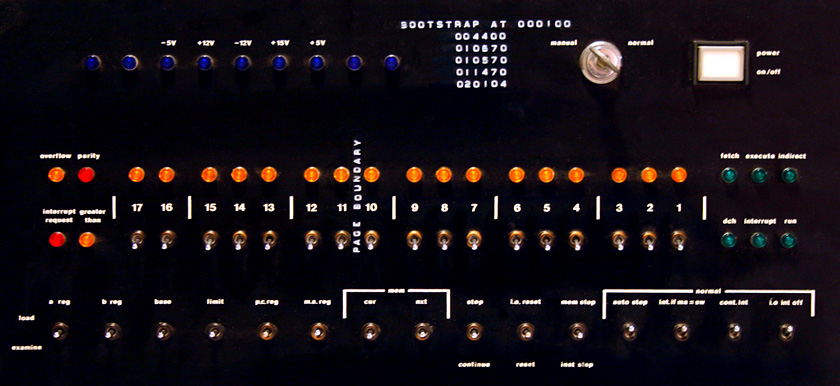
The BCL Molecular Control Panel
| 9x Blue Bulbs | Lit whilst the indicated voltage is present. |
| Keyswitch | Shown with the key inserted and turned to Manual.
|
| Power | On/Off Push Button, lit whilst the power is ON.
|
| overflow | Lit/Unlit according as the Carry flag is set/clear respectively. |
| parity | Lit whilst an uncleared Parity interrupt is requested.
|
| interrupt request | Lit whilst one or more interrupts are requested and unacknowledged. |
| greater than | Lit/Unlit according as the Greater than flag is set/clear respectively. |
| 17x Amber bulbs & switches | The 17 switches form the 17-bit Switch Register, shown here with all switches in the down position.
|
| 6x Green Bulbs | fetch, execute, indirect, data channel, interrupt, run. Lit whilst the designated CPU circuitry is busy, these bulbs twinkle merrily whilst the system is running normally.
|
| All 15 switches following are effective only when the keyswitch is set to manual | |
|---|---|
| The 11 switches following each have three positions: up, down or central (neutral) which automatically revert to neutral on release of finger pressure. | |
| 8x load/examine switches | a-register, b-register, base, limit, pc-register, ma-register, memory-current, memory-next.
|
| stop/continue |
|
| i.o.reset/reset |
|
| memory step/instruction step |
|
| All 4 switches following are two-position: central or down, shown in the central position (Normal). | |
| auto step | Down: the CPU will run at approximately five instructions per second. |
| interrupt if ma=sw | Down: the interrupt will be raised if, during CPU execution, MA-Register equals the value set on the SW-Register.
|
| continuous interrupt | Down: an interrupt will be raised after execution of every instruction.
|
| input/output interrupt off | Down: blocks interrupts from input/output devices.
|
Words
The Molecular word length is 17 bits. By convention, the bits are numbered B17:B1 from left to right and grouped into one pair (B17:B16) and five triples for representation in six octal digits, for example:
| 17 | 16 | 15 | 14 | 13 | 12 | 11 | 10 | 9 | 8 | 7 | 6 | 5 | 4 | 3 | 2 | 1 |
|---|---|---|---|---|---|---|---|---|---|---|---|---|---|---|---|---|
| 0 | 1 | 0 | 1 | 0 | 0 | 1 | 1 | 1 | 0 | 0 | 1 | 0 | 1 | 1 | 1 | 0 |
The above bit-pattern is written as 123456 in octal. All bits set is written as 377777 in octal.
In two's complement binary arithmetic, B17 is the Sign Bit. For numbers allocated more than one word, B17 in each low order word is never used. So a double word number has one sign bit followed by 32 binary digits (thus a double word -1 is stored as 377777 177777 in octal).
A word may hold two eight-bit Bytes: B16:B9 is called the Top Byte (octal Mask 177400) and B8:B1 is called the Bottom Byte (octal Mask 000377). B17 is spare:
| 17 | 16 | 15 | 14 | 13 | 12 | 11 | 10 | 9 | 8 | 7 | 6 | 5 | 4 | 3 | 2 | 1 |
|---|---|---|---|---|---|---|---|---|---|---|---|---|---|---|---|---|
| 0 | ||||||||||||||||
| TOP BYTE | BOTTOM BYTE | |||||||||||||||
Addresses
Each 17-bit memory word has a unique Memory Address of 16 bits (octal range 000000 to 177777), allowing 64K words to be addressed. A word is the smallest (and the largest) memory unit the instruction set can operate on (disc drive and line printer controllers can transfer larger blocks independently via a data channel).
Because Memory Reference Instructions are limited to the ten low order address bits (B10:B1), each 1K (210) boundary is very significant in programming and it is often useful to give each 1K memory block its own Page Number (in Octal of course, from 00 to 77). Thus the Memory Address 013004 may also be written as 05/1004 to indicate it is Word 1004 of Page 05. Indeed, this is the conventional way of indicating the presence of an absolute address.
Programs are handwritten in pencil on foolscap coding sheets, each sheet holding a "column" of 64 (decimal) memory words (or program "steps"). Thus the above address is sometimes also identified as Page 05 Column 10 Step 04:
| 17 | 16 | 15 | 14 | 13 | 12 | 11 | 10 | 9 | 8 | 7 | 6 | 5 | 4 | 3 | 2 | 1 |
|---|---|---|---|---|---|---|---|---|---|---|---|---|---|---|---|---|
| 0 | 0 | 0 | 0 | 1 | 0 | 1 | 1 | 0 | 0 | 0 | 0 | 0 | 0 | 1 | 0 | 0 |
| PAGE | COLUMN | STEP | ||||||||||||||
Registers and Flags
There are two General Purpose 17-bit registers available to programmers, known as the A-Register and the B-Register.
The A-Register has Memory Address 00/0000 and the B-Register has Memory Address 00/0001. So, to copy the A-Register to the B-Register you either store the A-Register at Memory Address 00/0001 or load the B-Register from Memory Address 00/0000.
The Carry Flag (the C-Flag) is a single bit accessible to programmers. It indicates a carry (or borrow) between B16 and B17 in Memory Reference addition (or subtraction) instructions and may participate in Register SHIFT and ROTATE instructions.
The Greater Than Flag (the GT-Flag) is a single bit accessible to programmers. The Memory Reference instructions CMPA and CMPB set (or clear) the GT-Flag according as the register (excluding B17) is (or is not) greater than the operand.
Do not rely on the hardware setting of the GT-Flag if the comparison may involve negative numbers!
The Switch Register (the SW-Register) is a row of 17 switches mounted on the Control Panel. Programs may read the SW-Register via the ESWRA and ESWRB instructions. The SW-Register may be set manually regardless of the position of the Control Panel's keyswitch.
The Program Counter (the PC-Register) holds the 16-bit Memory Address of the next instruction to be fetched for execution.
The Memory Address Register (the MA-Register) holds the 16-bit Memory Address of the Memory Word being read or written.
Instruction steps
The Processor executes an instruction as illustrated in the following flow chart, where the symbolic Instruction Register (IR) holds the 17-bit instruction under execution:
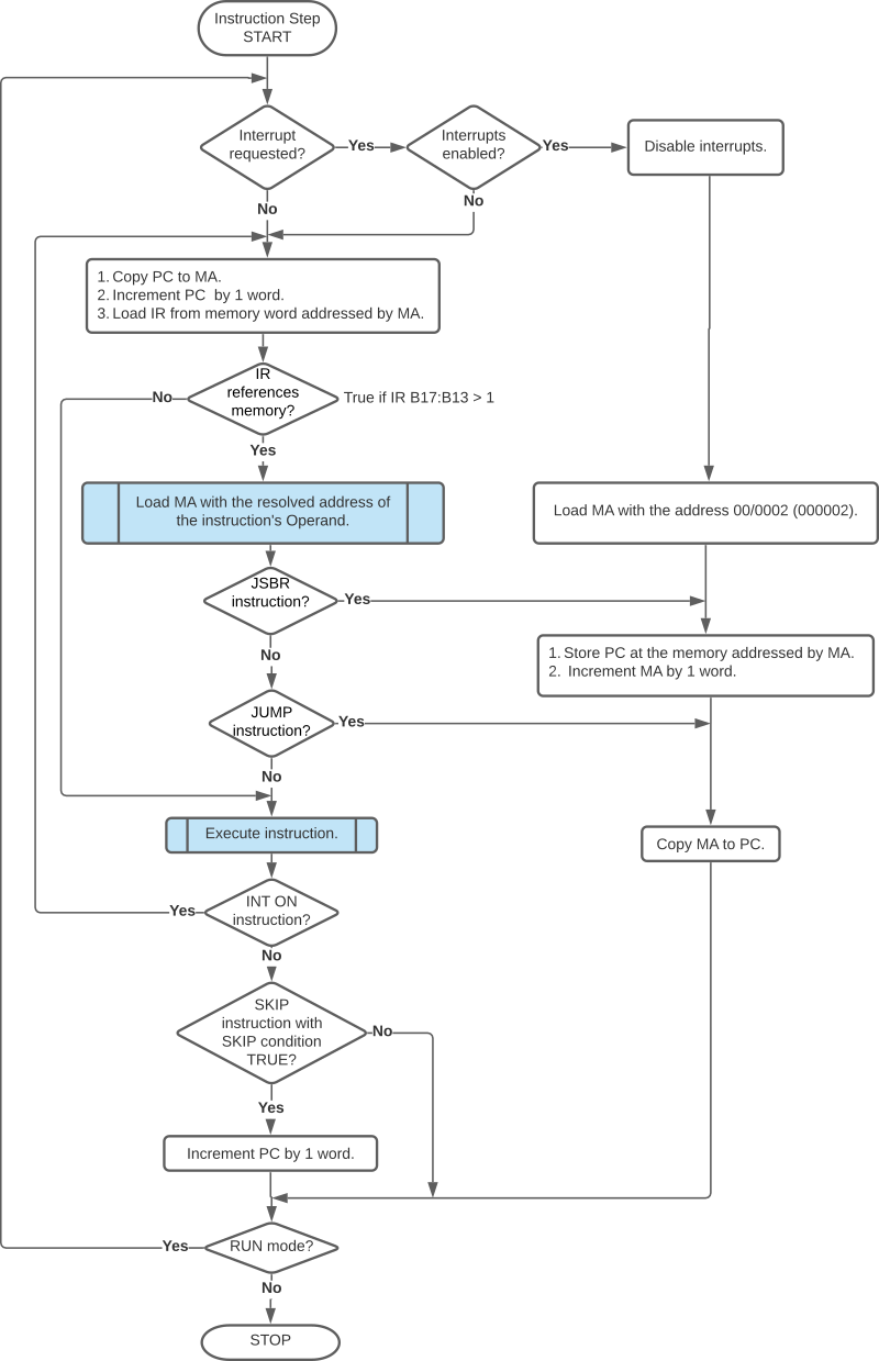
An interrupt is cleared when acknowledged by software. There is one interrupt level; further interrupts remain disabled until re-enabled by an Interrupt ON instruction, which takes effect only after the immediately following instruction (thus enabling the interrupt to be dismissed).
Interrupt priority is determined firstly by software, which should first test for MAINS OFF and ensure all interrupt service routines are kept short. Input/Output devices are grouped together by the Acknowledge Interrupt instruction with their relative priorities (probably) based upon the position of each interface board on the bus.
There is no stack. Subroutine calls are implemented by the JSBR instruction as shown above. Returns from subroutines (and interrupts) are accomplished via an indirect JUMP to the Return Address stored at the head of the subroutine.
At MAINS ON, MA and PC are loaded with the value 000002 and interrupts are disabled. Instruction execution will begin automatically if the control panel keyswitch is at NORMAL.
Privileged Instructions
These instructions (NOOP excepted) should be used only by the Operating System. The designation "privileged" is purely symbolic; there is no hardware protection to prevent their use by any application.
| 000000 | NOOP | No operation |
|---|---|---|
| 000001 | HALT | (requires manual resumption from Control Panel) |
| 000002 | MASK | Never used |
| 000003 | Acknowledge Interrupt | Loads B-Register with highest priority interrupting Device Code |
| 000004 | Interrupt ON | Enables interrupts after completion of the immediately following instruction |
| 000005 | Interrupt OFF | Disables interrupts |
| 000006 | Skip if Interrupt ON | Tests interrupt state |
| 000007 | Skip if Interrupt OFF | Tests interrupt state |
| 000010 | Skip if MAINS OFF | Tests and clears Mains Off interrupt |
| 000011 | Skip if MAINS ON | Tests and clears Mains On interrupt |
| 000012 | Skip if PARITY | Tests and clears Parity interrupt |
| 000013 | Skip if PROTECTION | Never used |
| 000014 | Skip if BOUNDARY | Never used |
| 000015 | Skip if MA=SW | Tests and clears MA=SW interrupt |
| 000016 | Skip if CONTINUOUS INTERRUPT | Tests and clear Continuous Interrupt |
| 000017 | Input/Output RESET | (allow 1 second for devices to react) |
Register Instructions
| 17 | 16 | 15 | 14 | 13 | 12 | 11 | 10 | 9 | 8 | 7 | 6 | 5 | 4 | 3 | 2 | 1 |
|---|---|---|---|---|---|---|---|---|---|---|---|---|---|---|---|---|
| 0 | 0 | 0 | 0 | 0 | 0 | 1 | 1=A reg 0=B reg | CLC | 1=LEFT 0=RIGHT | SHIFT | ROTATE | with CARRY | DEC | INC | SKIP if MSB=0 | SKIP if LSB=0 |
| 0 | 0 | 0 | 0 | 0 | 1 | 0 | 1=A reg 0=B reg | CLEAR | One's COMP | CLC | COMPC | SKIP | SWAP | CLEAR SIGN | COMP SIGN | ESWR |
| 0 | 0 | 0 | 0 | 0 | 1 | 1 | 1=A reg 0=B reg | 1=TRUE 0=FALSE | SKIP if NEG | SKIP if NOT 0 | SKIP if CARRY | CLC | SKIP if GT | CLGT | CLEAR | One's COMP |
Micro-Programming Rules
Instructions on the same row in the above table may be combined in a single instruction, subject to the following:
- Instructions will be executed in order from the left, except CLEAR SIGN which on some machines precedes CLEAR.
- If skips are combined, the skip will occur only if all conditions are fulfilled, except if AMSB and ALSB (or BMSB and BLSB) are combined the skip will occur if either or both conditions are met.
- The effect of combining SHIFT and ROTATE or INC and DEC is undefined.
For example:
005006 combines CLSA and COMPSA in that order to set the sign (B17) of the A-Register.
007502 combines AN0 and CLA to test for zero in, then clear, the A-Register.
| A-Register | B-Register | Instruction | ||
|---|---|---|---|---|
| 003001 | ALSB | 002001 | BLSB | Skip if B1=0 |
| 003002 | AMSB | 002002 | BMSB | Skip if B16=0 |
| 007600 | ANEG | 006600 | BNEG | Skip if B17=1 |
| 007500 | AN0 | 006500 | BN0 | Skip if not zero |
| 007200 | APOS | 006200 | BPOS | Skip if B17=0 |
| 007100 | A0 | 006100 | B0 | Skip if zero |
| 007002 | CLA | 006002 | CLB | Clear |
| 002400 | CLC | Clear CARRY Flag | ||
| 006004 | CLGT | Clear GREATER THAN Flag | ||
| 005004 | CLSA | 004004 | CLSB | Clear B17 (Sign bit) |
| 007001 | COMPA | 006001 | COMPB | Ones-Complement |
| 004040 | COMPC | Complement CARRY Flag | ||
| 005002 | COMPSA | 004002 | COMPSB | Complement B17 (Sign bit) |
| 003010 | DECA | 002010 | DECB | Decrement by one |
| 005001 | ESWRA | 004001 | ESWRB | Enter Switch Register (read Switches into) |
| 003004 | INCA | 002004 | INCB | Increment by one |
| 003240 | LRA | 002240 | LRB | Rotate Left by one (excluding B17) |
| 003260 | LRAC | 002260 | LRBC | Rotate Left by one including CARRY (excluding B17) |
| 001600+n | LRAn | 000600+n | LRBn | Rotate Left by n (excluding B17) |
| 003300 | LSA | 002300 | LSB | Left Shift by one (excluding B17) |
| 001700+n | LSAn | 000700+n | LSBn | Left Shift by n (excluding B17) |
| 003040 | RRA | 002040 | RRB | Rotate Right by one (excluding B17) |
| 003060 | RRAC | 002060 | RRBC | Rotate Right by one including CARRY (excluding B17) |
| 001400+n | RRAn | 000400+n | RRBn | Rotate Right by n (excluding B17) |
| 003100 | RSA | 002100 | RSB | Right Shift by one (excluding B17) |
| 001500+n | RSAn | 000500+n | RSBn | Right Shift by n (excluding B17) |
| 001520+n | RSAAn | 000520+n | RSABn | Right Shift by n Arithmetic |
| 001001 | SETGT | Set GREATER THAN Flag | ||
| 005006 | SETSA | 004006 | SETSB | Set B17 (Sign bit) |
| 006440 | SKC | Skip if CARRY Flag=1 | ||
| 006410 | SKGT | Skip if GREATER THAN Flag=1 | ||
| 004020 | SKIP | Skip unconditionally | ||
| 006040 | SKNC | Skip if CARRY Flag=0 | ||
| 006010 | SKNGT | Skip if GREATER THAN Flag=0 | ||
| 005010 | SWAPA | 004010 | SWAPB | Swap Bytes |
The maximum value of n is 15 (decimal).
Execution time 1.4 microseconds, except SETGT (1.2 μs) and multiple shifts/rotates (1.6 μs if n<=1; 3.2 μs if n<=6; 4.8 μs if n<=11; 6.4 μs otherwise).
Input/ Output Instructions
I/O instructions should only be executed by the Operating System or system software.
I/O devices may have up to three 17-bit Device Registers, accessible to the programmer, implemented by their hardware interface. By convention, Device Register 3 is the Status Register.
All I/O devices also have a BUSY flag and a DONE flag. Software starts a device by setting its BUSY flag (after loading relevant device registers); the device signals an INTERRUPT REQUEST whilst its DONE flag is set (unless disabled by the Current Mask).
| 17 | 16 | 15 | 14 | 13 | 12 | 11 | 10 | 9 | 8 | 7 | 6 | 5 | 4 | 3 | 2 | 1 |
|---|---|---|---|---|---|---|---|---|---|---|---|---|---|---|---|---|
| 0 | 0 | 0 | 0 | 1 | 1=A-Reg 0=B-Reg | FUNCTION or SKIP CONDITION | MODE | DEVICE CODE | ||||||||
Mode (B9:B7)
| B9:B7 | Mnemonic | Action |
|---|---|---|
| 1 | DATI1 | Read Device Register 1 |
| 2 | DATI2 | Read Device Register 2 |
| 3 | DATI3 | Read Device Register 3 |
| 4 | DATO1 | Write Device Register 1 |
| 5 | DATO2 | Write Device Register 2 |
| 6 | DATO3 | Write Device Register 3 |
| 7 | SKIP | Test for SKIP CONDITION |
Function or Skip Condition (B11:B10)
| B11:B10 | Function | SKIP IF |
|---|---|---|
| 0 | No Operation | BUSY |
| 1 | START (Set BUSY, Clear DONE) | NOT BUSY |
| 2 | STOP (Clear BUSY, Clear DONE) | DONE |
| 3 | IOPLS (Input/Output Pulse) | NOT DONE |
Device Codes (B6:B1)
| In | Out | Standard Assignment (M18 Mark 1 pre LOS) |
|---|---|---|
| 20 | 60 | Alpha-numeric Keyboard |
| 50 | 40 | Visual Display Unit |
| 30 | Line Printer | |
| 34 | Serial Printer | |
| 66 | 67 | IBM I/O Writer |
| 11 | 33 | Paper Tape |
| 70 | 70 | Disc |
Memory Reference Instructions
| 17 | 16 | 15 | 14 | 13 | 12 | 11 | 10 | 9 | 8 | 7 | 6 | 5 | 4 | 3 | 2 | 1 |
|---|---|---|---|---|---|---|---|---|---|---|---|---|---|---|---|---|
| OPERATION CODE | 0=Direct 1=Indirect | 0=Current Page 1=Zero Page | MEMORY ADDRESS | |||||||||||||
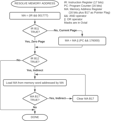 Memory Reference instructions can directly access memory only within the Current Page (i.e. the page within which the instruction itself is stored) or within the lowest Page (i.e. Page 00, often called Zero Page, comprising Words 00/0000 to 00/1777).
But that word may contain the 16-bit address of any word in memory and the Memory Reference instruction can indirectly access that word through the "pointer". If the pointer's B17 is set, then the target word is itself a pointer and so on indefinitely.
It's left to the programmer to ensure that such a chain does not form a closed loop.
| Operation Code | Mnemonic | Instruction | μ-sec |
|---|---|---|---|
| 02 | JUMP | Jump unconditionally | 1.2 |
| 03 | JSBR | Jump to Subroutine | 1.2 |
| 04 | INSZ | Increment by one, Skip if result is zero | 2.6 |
| 05 | DESZ | Decrement by one, Skip if result is zero | 2.6 |
| 06 | ANDA | AND into A-Register | 2.4 |
| 07 | IORA | Inclusive OR into A-Register | 2.4 |
| 10 | XORA | Exclusive OR into A-Register | 2.4 |
| 11 | ADA | Add to A-Register | 2.4 |
| 12 | ADB | Add to B-Register | 2.4 |
| 13 | SFA | Subtract from A-Register | 2.4 |
| 14 | SFB | Subtract from B-Register | 2.4 |
| 15 | ADAC | Add to A-Register with CARRY | 2.4 |
| 16 | ADBC | Add to B-Register with CARRY | 2.4 |
| 17 | SFAC | Subtract from A-Register with CARRY | 2.4 |
| 20 | SFBC | Subtract from B-Register with CARRY | 2.4 |
| 21 | LDA | Load into A-Register | 2.4 |
| 22 | LDB | Load into B-Register | 2.4 |
| 23 | CMPA | Compare with A-Register, Skip if B17:B1 unequal (see also GT-Flag) | 2.4 |
| 24 | CMPB | Compare with B-Register, Skip if B17:B1 unequal (see also GT-Flag) | 2.4 |
| 25 | STA | Store A-Register | 2.4 |
| 26 | STB | Store B-Register | 2.4 |
Each level of indirect addressing adds 1.2 μ-sec to the above instruction timings.
There is no hardware implementation of multiplication or division.
Disk Contamination - the size of the problem